The following content is from a very old report of a practical assignment I had to do when I was in my 2nd undergraduate year. It can contain a lot of errors. But here it is copied because information in this report might be helpful to students who just start learning about practical oscillator circuits in Electronics subjects.
This report has some figures/text directly taken from IC manufacturer datasheets and also from application notes provided with these ICs.
All the simulations were done using Electronics Workbench V5
Introduction
In the following experiments I implemented various oscillators and observed their characteristics. My focus was basically on sine wave generation techniques with TL084 QUAD OP-AMP IC and square wave generation using popular 555 IC.
Oscillator Definition
Oscillators are circuits that produce specific, periodic waveforms such as square, triangular, saw-tooth or sinusoidal. There are two main classes of oscillators: relaxation and sinusoidal. Relaxation oscillators generate the triangular, saw-tooth and other non-sinusoidal waveforms. Sinusoidal oscillators consist of amplifiers with external components used to generate oscillation or crystals that internally generate the oscillation.
Part I: Sine wave oscillators
Sine wave oscillators are used as references or test waveforms by many circuits. A pure sine wave has only a single or fundamental frequency. Ideally no harmonics are present.
Op-amp oscillators are circuits that are unstable. Oscillators are useful for generating uniform signals that are used as a reference in such applications as audio, function generators, digital systems, and communication systems.
Two general classes of oscillators exist: sinusoidal and relaxation. Sinusoidal oscillators consist of amplifiers with RC or LC circuits that have adjustable oscillation frequencies, or crystals that have a fixed oscillation frequency. Relaxation oscillators generate triangular, saw-tooth, square, pulse, or exponential waveforms.
Op-amp sine-wave oscillators operate without an externally-applied input signal. Instead, some combination of positive and negative feedback is used to drive the op amp into an unstable state, causing the output to cycle back and forth between the supply voltages at a continuous rate. The frequency and amplitude of oscillation are set by the arrangement of passive and active components around a central op amp. Op-amp oscillators are restricted to the lower end of the frequency spectrum because op amps do not have the required bandwidth to achieve low phase shift at high frequencies. Crystal oscillators are used in high-frequency applications up to the hundreds of MHz range.
Requirement for oscillation
Canonical Form of a Feedback System with Positive or Negative Feedback
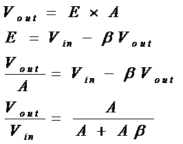
Here the simplest form of a negative feedback system is used to demonstrate the requirements for oscillation to occur. Figure 1 shows the block diagram for this system in which Vin is the input voltage, Vout is the output voltage from the amplifier gain block (A), and β is the signal called the feedback factor that is fed back to the summing junction. E represents the error term that is equal to the summation of the feedback factor and the input voltage.
Oscillators do not require an externally-applied input signal; instead, they use some fraction of the output signal created by the feedback network as the input signal.
Oscillation results when the feedback system is not able to find a stable steady-state because its transfer function can not be satisfied. The system goes unstable when the denominator in last equation becomes zero, i.e., when 1 + Aβ= 0, or Aβ= –1. The key to designing an oscillator is ensuring that Aβ= –1.
Satisfying this criterion requires that the magnitude of the loop gain is unity with a corresponding phase shift of 180° as indicated by the minus sign. This is called the Barkhausen criterion. For positive feedback configuration term Aβ=1 with 0° or 360° phase shift.
At this stage, one of three things can occur:
- Nonlinearity in saturation or cutoff causes the system to become stable and lock up at the current power rail.
- The initial change causes the system to saturate (or cutoff) and stay that way for a long time before it becomes linear and heads for the opposite power rail.
- The system stays linear and reverses direction, heading for the opposite power rail.
The second alternative produces highly distorted oscillations (usually quasi-square waves), the resulting oscillators being called relaxation oscillators. The third produces a sine-wave oscillator.
Wein Bridge Oscillator
The Wien Bridge is one of the simplest and best known oscillators. Figure shows the basic Wien Bridge circuit configuration. Advantages of the circuit are this circuit has only a few components and good frequency stability. The major drawback of the circuit is that the output amplitude is at the supply voltages, which saturates the op-amp and causes high output distortion.
Because this circuit uses both negative and positive feedback we have to derive an equation for the voltage gain of the amplifier. Here we first consider the positive feedback loop consisting of and to find V+. Then we consider the negative feedback path and find the Vout.
For Wein Bridge oscillator Z1=RG, Z2=RF, Z3=R+1/jω0, Z4=R||jω0 where ω0 is the oscillating frequency. Substituting in above equation we get. Therefore to satisfy the oscillation
voltage gain of the amplifier = 3 i.e. RF=2RG.
But practically if we design a circuit with voltage gain of exactly 3, oscillations does not begin automatically. To start the oscillations I used a switch witch momentarily connect inverting input of OP-amp to ground. This started oscillations but oscillation quickly decayed and stopped. Therefore to maintain sustained oscillations I had to use a voltage gain of at least 3.06. This can be explained because none of the components used are ideal and there is a loss of energy in RC networks, oscilloscope cables an op-amp itself.
Figure: The design of wein bridge oscillator (This design was used both for simulation and experiment)
Figure: Starting oscillations with a switch
Figure: Decaying Oscillations when gain is exactly 3
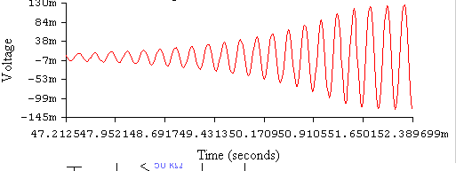
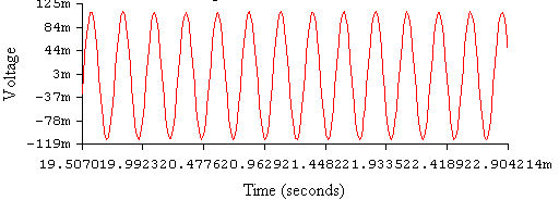
These facts caused us to use a voltage gain of more than 3 to keep oscillations and further higher gain to start oscillations (Oscillations start automatically due to noise). But there is a major drawback of using higher voltage gain. Higher the voltage gain, higher the distortion. Theoretically if voltage gain is more than 3 oscillations should not occur. But practically, since oscillator oscillates very close to supply rails, higher gain force the op-amp to a non linear region and it still oscillates producing remarkable distortion. This is illustrated in following pictures.
Figure: Stating oscillations automatically with higher gain.
Figure: Distorted wave forms
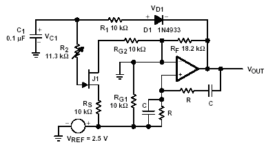
Solution: Use Automatic Gain Control
So to maintain an undistorted sine wave we have to use some form of an AGC with the amplifier gain. These can be done in two ways.
- Using non-linear feedback. We can use positive temperature coefficient device like a lamp for RG.
- Using a separate AGC feedback circuit.
Figure: Single supply Wein Bridge oscillator with AGC.
The Phase Shift Oscillator
The 1800 phase shift and the condition Aβ= 1 is introduced by active and passive components in any oscillator. In a phase shift oscillator we chose passive components to get the desired phase shift while keeping phase shift of active components constant. Since op-amps work best in low frequency spectrum RC networks are the preferred phase shift devices.
The following graph shows the phase shift introduced by RC networks with oscillating frequency. The rate of change of phase with frequency, dΦ/dω, determines frequency stability. When buffered RC sections (an op amp buffer provides high input and low output impedance) are cascaded, the phase shift multiplies by the number of sections, n.
So this graph shows us to get an 1800 phase shift we need at least two RC sections. But frequency stability is very low in such design. Therefore we use three RC sections. If we want to get good results we have to use buffered RC sections since RC sections can load each other causing higher voltage gain from the op-amp.
 Figure: The phase shift oscillator (This design was used both for the simulation and experiment.)
The normal assumption is that the phase shift sections are independent of each other.
Then using above Equation the loop phase shift is –1800, when the phase shift of each section is 600.
This occurs when ω=2πf = 1.732/RC because the tangent of 600 = 1.732.
The magnitude of β at this point is (1/2)3. So the gain, A, must be equal to 8 for the system gain to be equal to one.
- Therefore theoretical gain of op-amp = 8
- The practical gain to start an oscillation = 32.4
- The practical gain to keep oscillation = 31.6
- Theoretical frequency = 2.76 Khz
- Practical frequency = 3.78 Khz
The main reason for this is RC sections are not buffered. That is they load each other. Also the tolerance of the values of components can vary the results. But still there is a remarkable reduction in distortion comparing to the wein bridge oscillator.
Figure: Start of phase shift oscillator
Figure: Output of phase shift oscillator
Figure: Oscillation cease when gain reduces
Phase shift oscillator with buffered RC network.
The buffered phase shift oscillator is much improved over the un-buffered version. The buffers prevent the RC sections from loading each other; hence the buffered phase shift oscillator performs closer to the calculated frequency and gain. The gain setting resistor, RG, loads the third RC section. If the fourth buffer in a quad op amp buffers this RC section, the performance becomes ideal.
PART II: Square Wave Generation with 555 Timer.
The LM555/NE555/SA555 is a highly stable controller capable of producing accurate timing pulses. With monostable operation, the time delay is controlled by one external resistor and one capacitor. With astable operation, the frequency and duty cycle are accurately controlled with two external resistors and one capacitor.
The astable multivibrator:
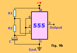
Astable operation: following figure shows the 555 connected as an astable multivibrator. Both the trigger and threshold inputs (pins 2 and 6) to the two comparators are connected together and to the external capacitor. The capacitor charges toward the supply voltage through the two resistors, R1 and R2. The discharge pin (7) connected to the internal transistor is connected to the junction of those two resistors.
When power is first applied to the circuit, the capacitor will be uncharged, therefore, both the trigger and threshold inputs will be near zero volts. The lower comparator sets the control flip-flop causing the output to switch high. That also turns off transistor T1. That allows the capacitor to begin charging through R1 and R2. As soon as the charge on the capacitor reaches 2/3 of the supply voltage, the upper comparator will trigger causing the flip-flop to reset. That causes the output to switch low. Transistor T1 also conducts. The effect of T1 conducting causes resistor R2 to be connected across the external capacitor. Resistor R2 is effectively connected to ground through internal transistor T1. The result of that is that the capacitor now begins to discharge through R2.
Figure: Astable Multivibrator
Frequency of operation
f = 1/(0.693C x (R1 + 2R2))
Off and On time periods
t1 = 0.693(R1+R2)C
t2 = 0.693 x R2 x C
And the duty cycle is
D = t1/t = (R1 + R2) / (R1 + 2R2) (This shows that D > 50)
Figure: AMV circuit 1 (Used both in simulation and experiment)
Figure: waveforms at Output and Capacitor
Astable Multivibrator II with 50% duty cycle
Even though it’s quite difficult to calculate the duty cycle of this AMV it can be shown that it can produce a duty cycle of 50%.
50% duty cycle gives
An interesting phenomena occurs when R1<=2R2 then AMV does not oscillate and remain on forever.
Figure: AMV with 50% duty cycle
Figure: AMV remains on when R1<=2R2
Astable multivibrator-III with adjustable duty cycle
Figure: AMV with 50% duty cycle(Here it can be adjusted to any value)
Frequency of operation
f = 1/(0.693 x C x (R1 + R2))
Duty Cycle
D = t1/t = R1 / (R1 + R2)
Figure: AMV waveforms (threshold voltage is distorted due to the non linearity of diodes.)
555 as a Voltage controlled Oscillator
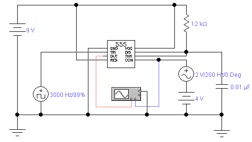
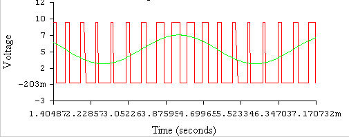
In this configuration a basic AMV is changed to work as a VCO using the control input of 555 IC. But there is one constraint. That is we cannot get larger frequency spectrum. Circuit has good linearity in the region it operates.
Figure: VCO (In experiment a function generator was used as the AC voltage source)
Figure: Output waveform and control voltage of VCO
Pulse Width Modulation using 555
Another two useful applications of 555 IC are PWM and frequency dividing. Both of these circuits are based on monostable operation of 555 IC. So the monostable mode of 555 is explained below.
Figure: The MMV block diagram
T = 1.1 x RC
Figure: The PWM circuit (this design was used for both simulation and experiment)
Figure: Output and control voltages of PWM
In this circuit there’s a considerable distortion in the actual circuit. In actual experiment when we change the control voltage not only the pulse width but the frequency of the output is also changed.
555 as a frequency divider
Figure: Schematic of the frequency divider circuit.
This circuit can be used to divide the frequency of a given pulse when the monostable time period is greater than the time period of the given pulse. This is shown in the following picture.
Figure: Output of the circuit with input
Reference: Sine Wave Oscillators, Texas Instruments

